Back
- Chemical vapor deposition (CVD)
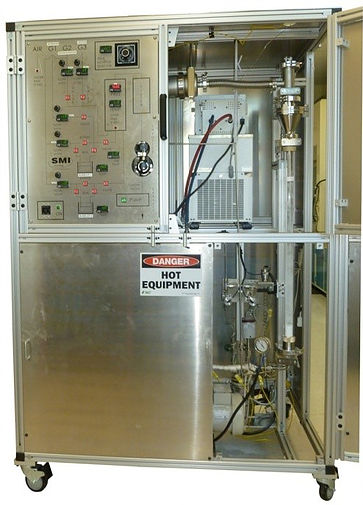
Chemical vapor deposition (CVD) is a chemical process used to produce high quality,
high-performance, solid materials. The process is often used in the
semiconductor industry to produce thin films.
Chemical vapor deposition (CVD) is a chemical process used to produce high quality, high-performance, solid materials. The process is often used in the semiconductor industry to produce thin films.
In typical CVD, the wafer (substrate) is exposed to one or more volatile precursors, which react and/or decompose on the substrate surface to produce the desired deposit. Frequently, volatile by-products are also produced, which are removed by gas flow through the reaction chamber.
Microfabrication processes widely use CVD to deposit materials in various forms, including: monocrystalline, polycrystalline, amorphous, and epitaxial. These materials include: silicon (SiO2, germanium, carbide, nitride, oxynitride), carbon (fiber, nanofibers, nanotubes, diamond and graphene), fluorocarbons, filaments, tungsten, titanium nitride and various high-k dielectrics.
CVD is commonly used to deposit conformal films and augment substrate surfaces in ways that more traditional surface modification techniques are not capable of. CVD is extremely useful in the process of atomic layer deposition at depositing extremely thin layers of material. A variety of applications for such films exist. Gallium arsenide is used in some integrated circuits (ICs) and photovoltaic devices. Amorphous polysilicon is used in photovoltaic devices. Certain carbides and nitrides confer wear-resistance.[7] Polymerization by CVD, perhaps the most versatile of all applications, allows for super-thin coatings which possess some very desirable qualities, such as lubricity, hydrophobicity and weather-resistance to name a few.[8] CVD of metal-organic frameworks, a class of crystalline nanoporous materials, has recently been demonstrated.[9] Applications for these films are anticipated in gas sensing and low-k dielectrics CVD techniques are adventageous for membrane coatings as well, such as those in desalination or water treatment, as these coatings can be sufficiently uniform (conformal) and thin that they do not clog membrane pores